Datasheets:
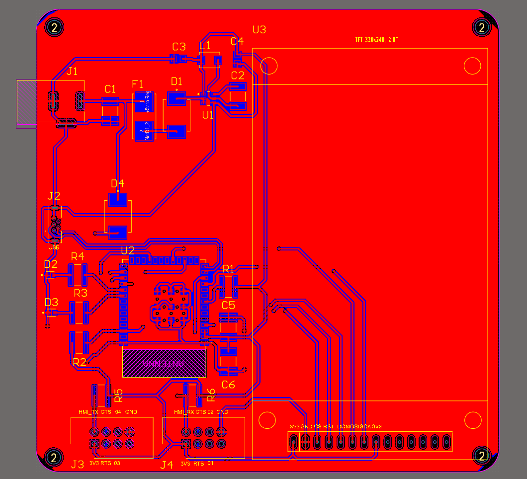
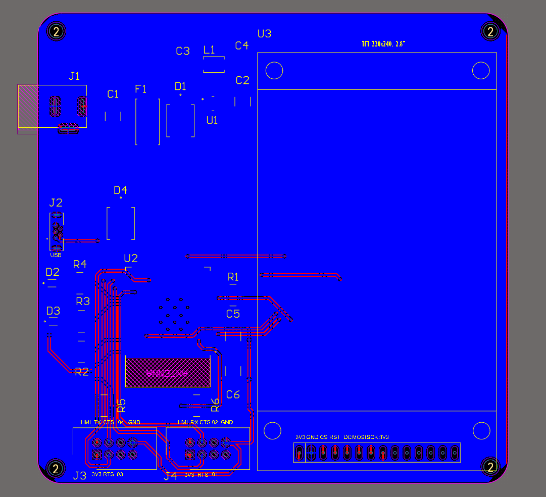
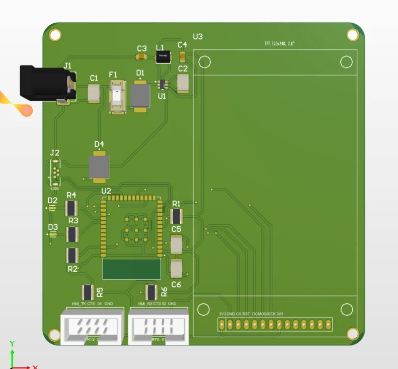
Schematic and PCB
Below is the Schematic and PCB, providing an overview of the components used in our system. This diagram also highlights how multiple perspectives were considered in designing the LCD module.
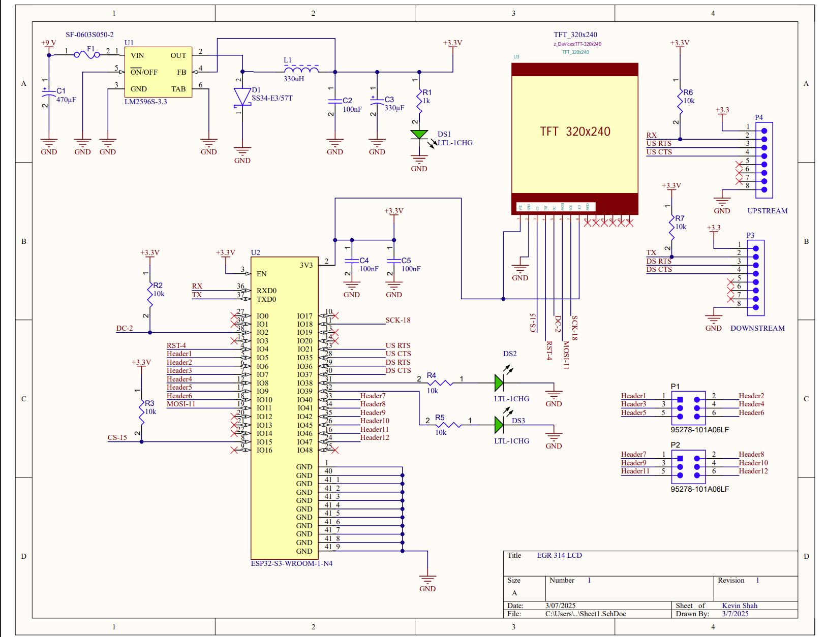
🔗 Schematic PDF
🔗 PCB PDF
E-Cad File
Gerber File
Schematic Functionality vs. Requirements
Our final HMI‐centric schematic brings together power, processing, user I/O, and communications into a single coherent PCB layout. Key functional elements include:
- Power Distribution & Regulation
- A 9 V barrel‐jack input feeds the AP63203WU-7 buck regulator, which provides a stable 3.3 V rail for all logic and peripherals.
- Decoupling capacitors and ferrite beads isolate the ESP32’s Wi-Fi bursts from sensitive sensor and display circuits.
-
This arrangement meets our requirement for reliable, low‐noise power under both high-current (LCD backlight, Wi-Fi) and low-current (sensors) modes.
-
Microcontroller & Peripheral Interfaces
- The ESP32’s UART pins are wired to the daisy-chain header, enabling both upstream sensor queries and downstream motor commands without additional multiplexers.
- SPI lines to the ILI9341 display (SCK, MOSI, CS, DC, RST) are laid out as short, impedance-controlled traces, ensuring fast, glitch-free updates (<50 ms) in response to new sensor frames.
-
I²C pins remain free for future local sensors, satisfying our scalability requirement.
-
User Controls & Feedback
- Two push-buttons routed to GPIO16/17 give users manual “Refresh” and “Override Flow” control, with 10 kΩ pull-ups and debounce capacitors ensuring clean, chatter-free inputs.
-
The 2.4″ TFT display is centrally placed and backlit via a dedicated MOSFET, providing clear, colorful real-time feedback for exhibit visitors.
-
Wireless Connectivity
- The ESP32’s antenna clearance zone and ground plane keep RF performance optimal, delivering robust MQTT connectivity for remote monitoring.
Together, these elements deliver on our product requirements for real-time local feedback, remote cloud updates, user-driven control, and educational transparency, all while maintaining a compact, single-board form factor.
Design & Decision‐Making Process for the Schematic
- Requirement Mapping
- We began by listing every functional requirement (power budget, UI responsiveness, communication paths, safety margins) and mapping them onto schematic blocks.
-
Power requirements drove regulator and decoupling choices; latency targets drove PCB trace layout for SPI/UART.
-
Component Footprint & Placement
- We grouped high-noise/high-current components (buck regulator, backlight MOSFET) away from analog lines.
-
The ESP32 was placed centrally to minimize trace lengths to both the daisychained UART header and the display connectors.
-
Signal Integrity Considerations
- SPI and UART lines were routed as differential‐like pairs with consistent trace impedance.
-
Pull-ups, series resistors, and ferrites were added to critical lines after lab-demo feedback showed occasional framing errors under load.
-
Iterative Feedback Incorporation
- After the first revision, TA feedback highlighted that our “Override Flow” button lacked proper debounce. We added a 0.1 µF capacitor and 10 kΩ resistor per channel.
-
Peer review noted Wi-Fi dropouts; we increased the antenna clearance area and added a ground-shield trace.
-
Validation & Final Checks
- We performed a DRC/DRU check in the CAD tool, then built a rapid prototype to verify power stability, button response, and display updates before freezing the schematic.
Version 2.0 Hardware Improvements
Looking ahead to a “Version 2.0” of this PCB, we would target the following enhancements:
- Integrated Sensor Daughter-Cards
- Why: Right now, external sensors connect via the I²C bus. Adding small mezzanine connectors for plug-in modules (e.g., BME280, light sensors) would simplify K-12 reconfiguration and reduce wiring errors.
-
Benefit: Increases the exhibit’s modularity and hands-on learning potential.
-
On-Board Motor Driver MOSFETs
- Why: Currently, motor control flows through the HMI board only as commands; a dedicated MOSFET stage on the HMI board would allow low-power test actuators (e.g., small fans) directly from this PCB.
-
Benefit: Enables standalone demo setups without needing the separate motor PCB.
-
USB-C Power & Debug Port
- Why: Switching from a barrel jack to USB-C PD would modernize the power interface and allow in-circuit debugging/programming via the same connector.
-
Benefit: Simplifies lab setup and future firmware updates, crucial for iterative educational projects.
-
Enhanced Display Touch Integration
- Why: Replacing the ILI9341 with a touch-capable TFT (e.g., FT81x series) would provide intuitive, touchscreen controls for data refresh and flow override.
-
Benefit: Improves user engagement and reduces the need for discrete buttons, streamlining the UX.
-
Power Monitoring & Telemetry
- Why: Adding current-sense resistors and an INA219/INA226 chip on the 3.3 V rail would let us monitor real-time power consumption and display it on the TFT or in the cloud dashboard.
- Benefit: Deepens the educational value by teaching students about power management and system diagnostics.
These Version 2.0 improvements build directly on our existing schematic footprint and trace layout, leveraging freed-up I²C lines and header pin reserves. They would further satisfy scalability, usability, and educational richness for future iterations.